But here’s a truth people outside the industry rarely consider: a single hidden solder issue in a PCB can bring an entire device to a halt. And because many of these defects can’t be seen with the naked eye, manufacturers need more than just good lighting and a microscope.
Enter X-ray inspection in PCB assembly—the behind-the-scenes hero of modern electronics manufacturing. Whether you work with an engineering team, follow manufacturing trends, or appreciate how precise today’s electronics have become, understanding X-ray inspection reveals why quality matters more than ever in PCB assembly.
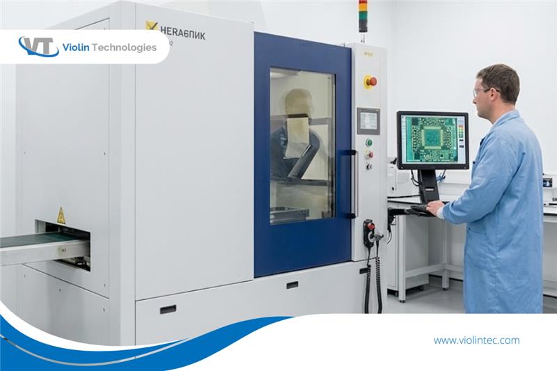
What Exactly Is X-Ray Inspection in PCB Assembly?
X-ray inspection is a non-destructive testing method preferably used to examine the internal features of a PCB without cutting it open. Instead of relying on visible inspection, X-rays penetrate the board and display hidden details such as:
- Solder joint quality
- Internal cracks
- Voids and air pockets
- Component misalignment
- Hidden BGA (Ball Grid Array) issues
- Barrel fill in through-hole components
This method is especially important in modern assemblies where components are shrinking, pads are hidden underneath chips, and density is increasing every year.
Why X-Ray Matters More Than Ever in Today’s Electronics
With the electronics industry rapidly evolving, PCB assemblies have become far more complex than they were a decade ago. More layers, more functionality, and tighter spaces mean more chances for defects to hide beneath the surface.
Here’s why X-ray inspection has become such a critical part of the process:
1. Hidden Solder Defects Are Now Common
In assemblies with bottom-terminated components, the solder joints are located beneath the device. You can’t inspect them visually because they’re not visible.
X-ray imaging reveals:
- Voids in solder
- Cold joints
- Solder bridging
- Incomplete wetting
These issues directly affect reliability, especially mission-critical products.
2. It Improves PCB Assembly Yields
Every electronics manufacturer wants to reduce rework, scrap, and unexpected quality failures. Accurate X-ray inspection becomes an essential tool for understanding PCB assembly yields, allowing engineering teams to pinpoint root causes and optimize the production process.
When you analyze where defects frequently appear, you’re better equipped to improve stencil design, reflow profiles, or pick-and-place accuracy.
3. It Supports Compliance with Industry Standards
Many companies today operate under strict customer and regulatory requirements. Whether you’re working to meet IPC standards for PCB assembly or adhere to industry guidelines, X-ray inspection provides the documentation and proof manufacturers need.
For example, IPC-A-610 and IPC-7095 emphasize proper BGA and solder joint verification—exactly the areas where X-ray plays a major role.
4. Essential for Medical, Aerospace, and High-Reliability Electronics
In industries where failure isn’t an option, X-ray inspection becomes non-negotiable.
Many customers look specifically for an ISO 13485 certified electronics manufacturer because they know medical electronics require fault-free assembly. X-ray imaging helps manufacturers meet these elevated expectations by catching inconsistencies before they ever reach the test stage.
What X-Ray Inspection Actually Reveals
To understand why it’s so important, let’s break down what X-ray tools uncover.
1. Voids in Solder
Tiny air pockets trapped inside solder joints weaken electrical and mechanical connectivity. Excessive voiding can cause heating, failure under load, or intermittent performance.
2. Insufficient Barrel Fill
Through-hole components need proper solder fill for long-term reliability. X-ray inspection shows exactly how much solder flowed into the vias—something no external camera can reveal.
3. Component Orientation
Misplaced, tilted, or misaligned components compromise signal integrity and function. X-ray highlights rotation errors or lifted leads instantly.
4. BGA Solder Ball Integrity
Each solder ball forms a critical junction between the PCB and the chip. A single defect can render the whole assembly useless. X-ray imaging maps out every ball so technicians can evaluate:
- Bridging
- Voids
- Cold joints
- Missing balls
- Short circuits

How EMS Providers Use X-Ray to Deliver Better Quality
Manufacturers around the world—especially high-end facilities—integrate X-ray systems into their inline or batch inspection process. Several of the top 10 EMS companies globally use automated X-ray systems (AXI) for high-volume production, as they enable real-time monitoring and batch traceability. Whether the assemblies are for consumer devices, aerospace electronics, industrial controls, or medical devices, X-ray inspection contributes to predictable quality and repeatable results.
Looking Ahead: X-Ray Technology Is Rapidly Advancing
The latest trends in X-ray inspection include:
- AI-powered defect recognition
- 3D tomography (CT) for multi-layer analysis
- Real-time inline inspection during reflows
- Higher resolution imaging for ultra-small solder joints
These advancements help teams detect issues earlier in the process, reducing scrap and improving yield.
As electronics continue to shrink and performance demands rise, the reliance on X-ray technology will only grow stronger.
Final Thoughts
X-ray inspection is no longer a “nice-to-have” step in PCB manufacturing—it has become a core requirement for building reliable, high-quality electronic assemblies. It helps manufacturers meet global standards, boost yield, and deliver products that perform consistently in real-world conditions.
Whether you work with a small batch manufacturer or one of the top 10 EMS companies, X-ray inspection is one of the most powerful safeguards you can have in your production workflow. It’s a direct reflection of commitment to quality, precision, and long-term reliability.