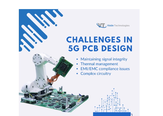
But, creating a PCB capable of managing high-speed signals has become a significant challenge for engineers. This blog post will examine key challenges in 5G PCB design and offer practical tips for overcoming them.
What we cover in this blog?
Key Takeaways
- Collaborate closely with manufacturers to ensure manufacturability and performance alignment.
- Optimize signal integrity through meticulous routing and impedance control.
- Manage thermal challenges with strategic use of thermal vias and active cooling.
- Ensure EMI/EMC compliance with effective grounding and shielding techniques.
Challenges In 5G PCB Design
Challenge 1: Maintaining signal integrity
Optimal signal integrity is paramount in high-speed printed circuit board design, ensuring signals maintain their quality during transmission. High-speed signals are vulnerable to noise and crosstalk, leading to degradation and data loss. Thus, preserving signal integrity throughout the PCB design process is critical.
Solution: To address this, designers should prioritize meticulous planning and layout optimization, which involves refining routing, ground and power planes, and integrating decoupling capacitors. Employing signal integrity simulation tools helps in identifying and resolving potential issues prior to PCB fabrication.
Challenge 2: Thermal management
High-frequency signals in high-speed PCBs generate a lot of heat, which can lead to component overheating and subsequent performance and reliability issues.
Solution: To address this challenge, designers should employ thermal vias, pads, and relief pads strategically to dissipate heat effectively. Furthermore, a blend of active and passive cooling methods, like heat sinks and fans, should be considered to mitigate temperature rise and ensure optimal PCB operation.
Challenge 3: EMI/EMC Compliance
High-speed printed circuit board design faces significant challenges related to electromagnetic interference (EMI) and electromagnetic compatibility (EMC) compliance. EMI disrupts electronic device performance by unwanted electromagnetic energy, while EMC compliance ensures devices do not emit excessive electromagnetic energy that interferes with others.
Solution: To address EMI/EMC challenges, designers should adhere to grounding and shielding best practices, including optimal component placement and effective filtering methods. Also, to deal with cross talk due to analog and digital frequencies, separating the traces is highly preferable. Utilizing ferrite beads or inductors to mitigate high-frequency noise is also recommended.
Challenge 4: Complex Circuitry
The growing complexity and density of circuitry pose significant challenges for manufacturers in PCB fabrication today. To support the higher data rates and multiple-input, multiple-output capabilities of 5G, PCBs need to integrate more components into smaller spaces.
Solution: Advanced PCB design techniques such as microvia technology and multilayer PCBs are essential. These techniques are crucial for maintaining signal integrity and reducing electromagnetic interference (EMI), making them indispensable for modern printed circuit board designs.
Challenge 5: Design for Manufacturing
Manufacturing high-speed PCBs poses challenges due to fine-pitch components and high-density interconnects.
Solution: To address manufacturing challenges, collaboration between designers and manufacturers is crucial. While designing PCBs, designers should ensure that the design adheres to standard rules, including trace width and spacing specifications. It’s also essential to avoid components that are challenging to place or solder, ensuring smooth and efficient manufacturing processes.
Addressing these challenges requires a combination of advanced design techniques, careful material selection, precise manufacturing processes, and thorough testing and validation monitored by experts such as electromechanical assemblies and box-build manufacturers.

Tips for 5G Printed Circuit Board Design
Understand the requirements
Familiarize yourself with the various frequency bands and ranges used in 5G. Understand the importance of signal integrity in high-frequency designs and the impact of various factors such as trace width, spacing, and via design.
Material selection
Use PCB materials with higher thermal conductivity and low dielectric loss to reduce signal attenuation. Select materials with superior thermal conductivity while preserving consistent electrical properties across a broad temperature and frequency range by leveraging the expertise of a contract manufacturing company in Chennai.
Advanced simulation tools
Use electromagnetic (EM) simulation tools to model and predict signal behavior, impedance, and potential EMI issues. Perform thoroughly mixed-signal design and integrity analysis using tools like HFSS, CST, or ADS to optimize the design to produce precise trace lines.
Impedance control
Design controlled impedance traces to match the characteristic impedance required by high-frequency signals. Carefully design the PCB layer stack up to ensure uniform impedance and minimize signal degradation.
Thermal management
Incorporate heat sinks, thermal vias, and proper copper pours to dissipate heat effectively. Use thermal simulation tools to predict and manage signal propagation speed, heat distribution, and low dielectric constant.
Routing techniques
Use microstrip and stripline routing techniques to maintain signal integrity. Avoid sharp 90-degree turns in traces; use mitered or curved paths with thinner traces to reduce signal reflection.
Via design
Minimize the number of vias in high-frequency signal paths to reduce signal loss and reflection. Use back drilling to remove stubs and reduce via impedance in transmission lines or AC and DC circuits.
EMI/EMC considerations
Implement shielding techniques to ensure EMC compliance. Use solid ground planes to provide a return path for high-frequency signals and reduce EMI.
Testing and validation
Use advanced equipment capable of measuring high-frequency performance. Build and test prototypes to validate design assumptions and performance before full-scale production.
Continuous learning
Stay updated on 5G technology and PCB design practices via courses, webinars, and industry publications. Collaborate with other engineers and engage in discussion forums to share industry knowledge and learn from others’ experiences.
Documentation and standards
Maintain detailed documentation of your circuit board design process, including material specifications, simulation results, and testing procedures.
By implementing these hacks and continuously improving your knowledge and skills, you can master the complexities of 5G PCB design and produce reliable, high-performance circuit boards used for advanced communication systems.
Contract manufacturers in India possess the required expertise to achieve industry standards.
Conclusion
Designing 5G PCBs presents challenges, but with meticulous planning, adherence to grounding and shielding best practices, implementation of thermal management strategies, and collaboration with manufacturers, designers can conquer these obstacles. This approach ensures the creation of high-performance, dependable PCBs that align with the requirements of modern high-speed digital communication technologies.
Frequently Asked Questions
What are the main challenges in designing high-speed PCBs?
Designing PCBs of high speed involves challenges such as maintaining signal integrity, managing thermal issues, ensuring EMI/EMC compliance, and handling the complexity of dense circuitry.
How can signal integrity be preserved in high-speed PCB designs?
Signal integrity can be preserved by optimizing trace routing, minimizing impedance mismatches, using controlled impedance traces, and employing signal integrity simulation tools to analyze and refine designs.
What thermal management techniques are effective for high-speed PCBs?
Effective heat management techniques include using thermal vias, thermal pads, and relief pads for heat dissipation, as well as integrating active cooling solutions like heat sinks and fans to prevent component overheating.
What role does collaboration with PCB manufacturers play in designing 5G PCBs?
Collaboration with PCB manufacturers ensures that designs are manufacturable and meet performance requirements. It involves following manufacturing guidelines, choosing suitable materials, and addressing assembly challenges early in the design process.

Aparna Sushumna
About the Author
Aparna Sushumna, a mother to a hyperactive toddler who is all over the house. I aspire to be a decent content developer. A Bachelorette of technology says my qualification but I anticipated being a singer. Thanks to the recession, I dwelled into various jobs, from coding to being a tech support executive to a help desk professional, only to conclude that there is something else I wish to do. Here I am to accomplish my profound passion for content writing. Music, nature, jewelry, beauty, mythology, life quotes, celebs, and their life, being my areas of interest.

